In the rapidly evolving world of #SemiconductorWaferFabrication, the year 2025 marks a pivotal moment characterized by a remarkable blend of innovative techniques and strategic foresight. As technology advances at an unprecedented pace, the landscape of wafer fabrication is undergoing significant changes, necessitating a deep and nuanced understanding of current trends to maintain competitiveness in this dynamic field. Companies operating within the semiconductor sector must not only recognize these shifts but also adopt trend-driven strategies that will ensure they remain at the forefront of technological advancements. As the demand for semiconductors grows in various sectors, including consumer electronics, automotive, and emerging fields like artificial intelligence, it becomes increasingly vital for firms to innovate and adapt continuously.
Key Techniques for Advanced Wafer Fabrication
Advanced Semiconductor Wafer Fabrication Techniques 2025
The landscape of advanced semiconductor wafer fabrication is undergoing a profound transformation as we move through 2025. #ModernTechniques, driven by new technologies and methodologies, are reshaping the industry, and the advancements made so far are contributing to greater efficiency and precision. For instance, the incorporation of advanced etching and deposition methods allows for finer features on wafers, leading to better performance capabilities in the final products. The integration of these new methods is vital for operations that aim to produce high-quality wafers with reduced resource consumption and greater output. As competition intensifies, companies that harness these advanced techniques will not only gain a competitive advantage but also contribute to a more sustainable manufacturing ecosystem by minimizing waste and optimizing resources.
Next-Gen Semiconductor Fabrication Process Innovations
Innovation is at the core of the next-generation semiconductor #FabricationProcesses. These innovations set new industry standards in manufacturing, allowing companies to significantly improve yield rates and operational efficiency. In real-world applications, these advancements have led to tangible successes, enabling manufacturers to overcome previous limitations and achieve unprecedented levels of performance. For example, techniques such as Extreme Ultraviolet (EUV) lithography are revolutionizing chip design and production capabilities, facilitating the fabrication of chips with more complex architectures. This leap in capability not only reflects technological prowess but also aligns with the increasing demands for higher computational power in consumer and industrial applications alike.
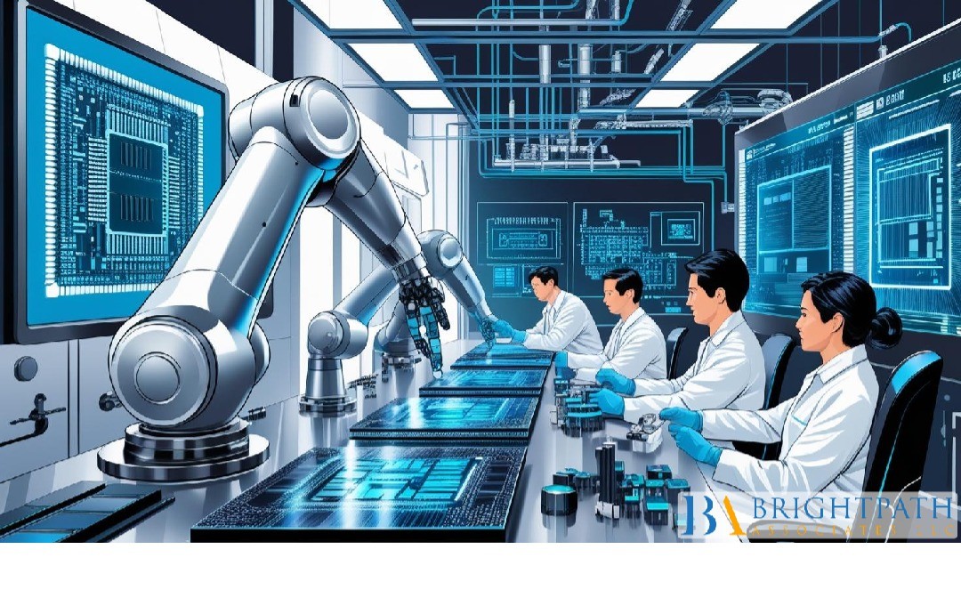
AI-Driven Wafer Production Optimization
#ArtificialIntelligence (AI) is playing an increasingly transformative role in wafer production optimization. By leveraging AI algorithms, manufacturers can enhance production outcomes significantly, focusing on improving quality control and significantly accelerating production processes. With AI-driven solutions that facilitate real-time decision-making, manufacturers are equipped to dynamically adjust processes to maintain peak efficiency. Sophisticated data analyses allow for predictive maintenance, ensuring that equipment runs smoothly and downtime is minimized. Furthermore, AI can identify patterns and anomalies within production data that human operators may overlook, leading to continuous improvements and innovation in production techniques.
Strategies for Excellence in Chip Manufacturing
High-Precision Photolithography in Semiconductor Fabrication
High-precision photolithography continues to be central to achieving excellence in chip manufacturing. Recent developments in photolithography technology have significantly pushed the boundaries of achievable precision, which is critical for facilitating the creation of smaller nodes with enhanced capabilities. The implications for precision in photolithography are vast, involving improvements not only in energy efficiency but also in performance in end-use applications such as mobile devices and high-performance computing. As chips become more complex and compact, the necessity for impeccable photolithographic processes becomes even more pronounced, highlighting the intricate relationship between technological advancement and manufacturing capability.
Cleanroom Standards for Advanced Semiconductor Fabs
The evolution of #CleanroomTechnology and standards continues to uphold the intricate requirements of advanced semiconductor fabs. Maintaining strict cleanroom standards is essential for controlling contamination, which is critical for the reliability and consistent performance of semiconductor devices. Given the sensitive nature of semiconductor manufacturing processes, even the slightest contamination can lead to product failures and significant losses. The role of cleanrooms has never been more critical, with evolving technological demands necessitating stringent control measures. This commitment to excellence in cleanroom standards forms the backbone of the semiconductor manufacturing ecosystem, ensuring that companies can deliver consistent quality.
Automated Semiconductor Fabrication Technologies
Automation within semiconductor fabrication is transforming how production processes are structured and optimized. By utilizing automated systems, manufacturers maximize efficiency and significantly reduce the potential for human error. The integration of smart technologies, such as advanced robotics and machine learning technologies, is ushering in a new era of manufacturing that promises numerous benefits. These systems provide precise control over fabrication processes, contributing to more consistent output and improved product quality. Furthermore, automation can enhance scalability, allowing manufacturers to adjust production levels swiftly to meet fluctuating market demands without compromising quality.
Best Practices in Semiconductor Process Control
Establishing best practices in #SemiconductorProcessControl is pivotal for maintaining optimal process conditions throughout the manufacturing lifecycle. Employing continuous monitoring techniques enables manufacturers to ensure superior outcomes by maintaining stringent oversight over every stage of production. This proactive approach helps identify potential issues early, allowing for timely corrective measures to be implemented before they escalate into more significant problems. Adopting a culture of continuous improvement and embracing technological advancements in monitoring and control systems will further enhance a manufacturer’s ability to produce high-quality semiconductor products efficiently.
Exploring Future Trends in Semiconductor Fabrication
Emerging Materials in Semiconductor Wafer Manufacturing
Innovations in #MaterialScience are driving significant performance gains in semiconductor manufacturing. Exploring new and emerging materials helps manufacturers to leverage unique properties that can significantly enhance technology-driven advancements. For instance, the development and adoption of materials such as graphene and advanced silicon compounds hold the potential to revolutionize chip performance, allowing for faster processing speeds and greater power efficiency. Analyzing these materials provides critical insights into how they may impact future technologies, influencing the evolution of the semiconductor industry’s landscape in profound ways.
Future Trends in Semiconductor Wafer Fabrication Industry
Looking toward the future, numerous trends are shaping the trajectory of the semiconductor fabrication industry. Projections indicate a continued emphasis on sustainability, with companies increasingly recognizing its importance not only as a corporate responsibility but also as a competitive necessity. Sustainable practices, including the reduction of #EnergyConsumption and waste, not only support environmental goals but can also enhance operational efficiency and long-term resilience. Furthermore, as global regulations surrounding sustainability tighten, companies that have already adopted eco-friendly practices will have a distinct advantage in compliance and public perception.
Executive Search for Leading Industry Talent
The competitive landscape of semiconductor wafer fabrication underscores the essential role of executive leadership in driving innovation and achieving excellence. Effective strategies for #ExecutiveSearch and talent acquisition ensure that organizations have the right leadership necessary to navigate the complexities of this industry. By focusing on the recruitment of top talent with specialized skills and visionary perspectives, companies can foster a culture of innovation that will allow them to maintain a competitive edge. As technology continues to advance, securing leaders who can imagine and implement the next significant breakthroughs will be crucial for long-term success.
Conclusion
In conclusion, the semiconductor wafer fabrication industry is poised for #SubstantialGrowth and transformation in the coming years. Embracing cutting-edge techniques and strategic imperatives is not merely advantageous; it is essential for staying ahead of the competition. Companies that possess the agility to navigate these changes and innovate effectively will be well-positioned to capitalize on the myriad opportunities presented by this dynamic field. As such, the call to action is clear: embrace innovation, invest in talent, and leverage strategic insights to drive future success in semiconductor fabrication, ensuring a robust and resilient industry that can meet the demands of tomorrow.
Find your next leadership role in Semiconductor Industry today!
Stay informed with the latest insights on Semiconductor Industry!